In the world of high-speed networking, the spotlight often shines on the incredible silicon feats: the multi-terabit Ethernet Switch ASICs, the advanced 800G PHY integration, and PAM4 signaling. Yet these capabilities are inert without the software and firmware layers that configure, control, and observe them. Software defines behavior, silicon enforces it.
This article delves into the intricate relationship between hardware and software, examines some of the interfaces and control paths that transform an ASIC into a functional network element.
1. Network Intelligence: Data, Control, and Management Planes
Switch operation is broadly structured around three planes,
- The Data Plane (Forwarding Plane): Implemented in ASIC hardware. Executes deterministic packet forwarding at line rate using pre-installed entries in TCAM, SRAM, or on-chip pipelines.
- The Control Plane: Runs on the Host CPU. Maintains topology and routing state through protocols such as BGP, OSPF, and IS-IS. Generates the forwarding entries that are programmed into hardware.
- The Management Plane: Provides operational visibility and configuration through APIs and management protocols (SSH, SNMP, NETCONF/YANG, and gNMI). Often integrated with automation frameworks or orchestration systems. It allows network operators and automated systems to configure VLANs, define QoS policies, monitor performance, and troubleshoot issues.
Synchronization between Control and Data planes defines overall switch responsiveness. The Management plane serves as the northbound interface to human or automated controllers.
2. Switch SDK: The Software Abstraction Layer
The Switch Software Development Kit (SDK) is the boundary between the Network Operating System (NOS) and the hardware. It is implemented as a set of user-space libraries and kernel drivers, often proprietary and tightly coupled to the ASIC’s internal microarchitecture.

Core functions:
- Abstraction: Exposes a logical API to the NOS (e.g. SONIC, proprietary vendor OS), insulating upper layers from ASIC-specific register maps and microcode sequences
- Translation: It translates high-level NOS commands (e.g., “create VLAN 10,” “add route to 192.168.1.0/24”) into the precise sequence of internal control interface commands and register writes that program the ASIC’s internal tables (like TCAM for route lookups or SRAM for MAC addresses)
- DMA Coordination: It manages the DMA engines for efficient packet handling and statistics collection
- Resource Management: Handles allocation and synchronization for shared hardware resources (queues, counters, buffer pools)
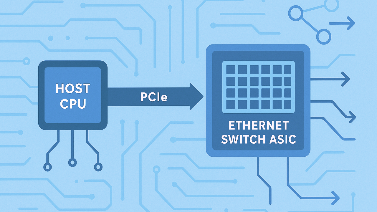
3. The PCIe Interface: Connecting the Host CPU to the ASIC
PCIe serves as the high-bandwidth, low-latency communication conduit, allowing the CPU to connect, manage and control the ASIC efficiently.
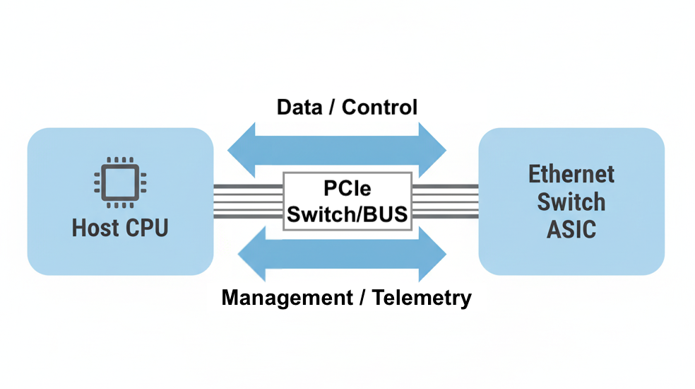
This connection facilitates two primary functions:
- Memory-Mapped I/O for Configuration: The CPU accesses the ASIC’s internal registers (for configuration, status, and control) by mapping them into its memory space. A write to a specific memory address by the CPU translates into a register write on the ASIC, configuring anything from port speed to VLAN membership
- Packet Punting (The “Slow Path”): Not all packets are handled at line rate by the ASIC. Packets that require complex software processing (e.g., protocol negotiation packets for ARP, BGP, OSPF hellos, or packets with an expired TTL) are flagged by the ASIC and efficiently transferred – or “punted” – over the PCIe link to the Host CPU’s memory for software-based handling. This defines the “Slow Path” where software intervenes for exceptions
4. The Side Channel and DMA: Internal Communication within the ASIC
While PCIe handles the external communication between the CPU and the ASIC, inside the ASIC, the configuration and data movement rely on two key subsystems.
- The Side-Channel Bus: This is a dedicated internal communication bus within the ASIC. It acts as the central messaging conduit for all configuration and management commands. When the CPU writes to a register or attempts to program a forwarding table entry via PCIe, that command is translated into an Side-Channel message. This message then travels on the internal Side-Channel bus to the specific functional block within the ASIC (e.g. ingress parser, lookup engine, egress scheduler) that needs to be programmed or queried. The Side-Channel provides arbitration, ordering, and acknowledgments
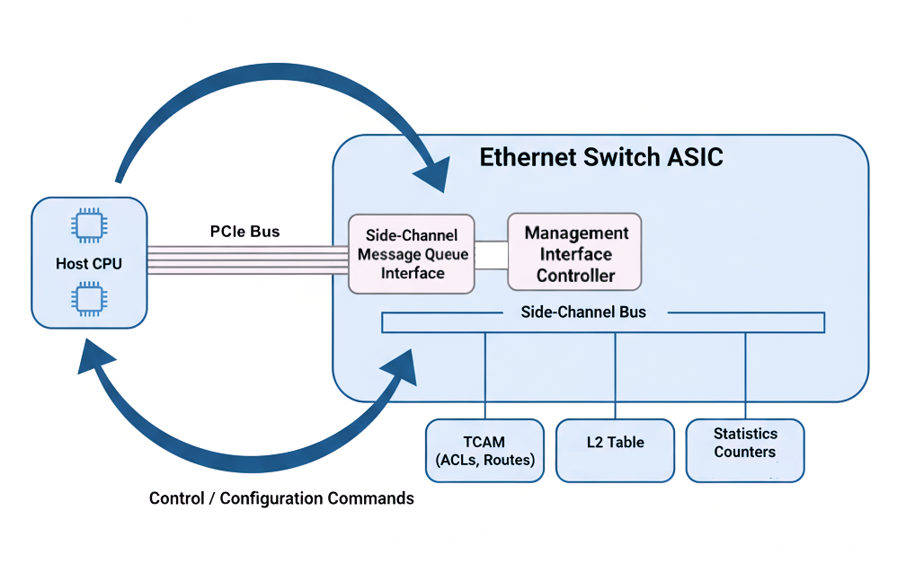
- The Direct Memory Access (DMA) Engine: Executes bulk transfers between ASIC memory (packet buffers, counter tables) and host memory. DMA operations offload the CPU by enabling Packet Injection/Punting: Bidirectional movement of packets between the NOS and ASIC and Statistics Collection: Periodic DMA reads of statistics, buffer utilization, and error counters to host memory or directly to an in-band telemetry pipeline
High-end ASICs implement multiple DMA channels to isolate traffic classes (control, telemetry, management).
5. Managing the Edge: PHYs and Optical Modules
The ASIC interfaces with external PHYs and optical transceivers that terminate physical links. Software manages these through standards based sideband buses.
- MDIO/MDC for PHY Configuration: The Host CPU or the Switch ASIC uses the MDIO/MDC (Management Data Input/Output/Clock) interface, an IEEE standard, to communicate directly with external PHY chips. This low-speed, two-wire bus is used to configure port speeds, initiate Link Training (critical for PAM4 signaling), and read basic link status.
- I2C and CMIS for Optical Modules: For sophisticated optical transceivers, the I2C interface, governed by specifications like CMIS (Common Management Interface Specification), allows the software to:
- Link Scan Thread: The SDK typically implements a link scan thread to continuously monitor physical link states across all ports.
6. Telemetry and Observability
Modern switches implement fine-grained telemetry through on-chip firmware, counters, packet samples, and streaming export via gNMI or INT (In-band Network Telemetry). The SDK configures hardware collectors, while DMA and PCIe provide export transport. Real-time telemetry enables adaptive traffic engineering and failure localization.
7. System Integration Considerations
Designers must account for:
- Latency Budget: PCIe latency and Side-Channel turnaround time responsiveness.
- Synchronization: Multi-threaded access to shared ASIC tables must be serialized or protected by SDK primitives.
- Error Propagation: Software must surface parity errors, ECC faults, and DMA timeouts via structured interrupts or event queues.
- Thermal and Power Management: Control-plane software typically interfaces with embedded controllers over I²C/PMBus for fan, voltage, and thermal regulation
Conclusion:
Switch silicon delivers forwarding capacity, firmware and software deliver operability. The Control and Management planes, ASIC SDK, PCIe transport, and internal buses collectively define the architecture’s control topology.
For principal engineers and architects, deep understanding of these internal buses and interfaces is foundational to designing scalable, programmable, and observable switching systems.
Leave a Reply