The shift from 1G copper to 400G/800G PAM4 is not a mere incremental upgrade but a complete re-architecture of the network interfaces. For engineering teams building next-gen switches and PHYs the challenge has evolved. It is no longer about optimizing a single PHY chip. Today, it is about orchestrating a distributed electrical-optical system where every component is a point of optimization and a potential failure.
1G Copper PHY: Simple and Self Contained
In the 1G era, the PHY was a simple, monolithic chip.
- Architecture: The entire PHY (PCS, PMA, PMD) was integrated into a single chip. It handled the electrical-to-electrical conversion and connected directly to a copper cable via an RJ45 jack
- Signaling: It used NRZ (Non-Return-to-Zero) signaling. This was a simple and robust “on/off” method that did not require complex signal processing
- Protocols: Auto-negotiation and link training process did not require iterative physical-layer calibration
- The System Interface: The interface between the switch ASIC and the PHY chip was usually simple GMII or SGMII, reliable, and easy to design

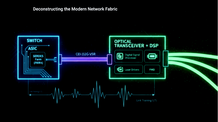
The 400G Optical Transceiver: A Distributed, Intelligent System
The PHY is now split across two physical domains, the electrical domain on the main ASIC and the optical domain in the pluggable module.
- Architecture: The PCS and PMA (SERDES) are on the main switch ASIC, while the PMD and a powerful DSP are inside the transceiver. The DSP handles the PAM4 signaling, performs Forward Error Correction (FEC), and manages the iterative Link Training process. This makes the transceiver a highly intelligent component, not just a converter
- Signaling: It uses PAM4 (4-level Pulse Amplitude Modulation). This doubles the data per lane but makes the signal fragile and susceptible to noise. This single change necessitated a total re-architecture of the PHY
- Protocols: The process is a two-step dance. a preliminary Auto-Negotiation (AN) followed by a mandatory, iterative Link Training (LT) calibration. The DSP in the transceiver’s PMD actively tunes the signal to compensate for the cable’s impairments. (Note: For very short-reach optics like SR, link training may be minimal.)
- The System Interface: The interface between the switch ASIC and the transceiver is a high-speed Common Electrical I/O (CEI) interface (e.g., CEI-112G-VSR). Each lane requires careful engineering to maintain signal integrity at 112G PAM4 speeds

The Road Ahead: From Plug-and-Play to Engineered Systems
The transition from copper to optical links has demanded a holistic, system-level design approach. It’s no longer just about designing a better chip. It’s about designing a seamlessly integrated electrical-optical system where the physical link is an active, intelligent part of the solution. The next frontier, Co-Packaged Optics (CPO), will further integrate these components, pushing the limits of power efficiency and bandwidth density.
Takeaway:
The jump from 1G copper to 400G/800G PAM4 is not just about faster bits. It is about distributing the intelligence, system-wide optimization and rethinking what a “PHY” really means. For Engineers, system designers and VPs, it is a reminder that simplicity at a chip level no longer guarantees simplicity at the system level.
Leave a Reply